イベント情報
【GIR公開セミナー】Dr. Michał Boćkowski / ポーランド科学アカデミー (ポーランド)
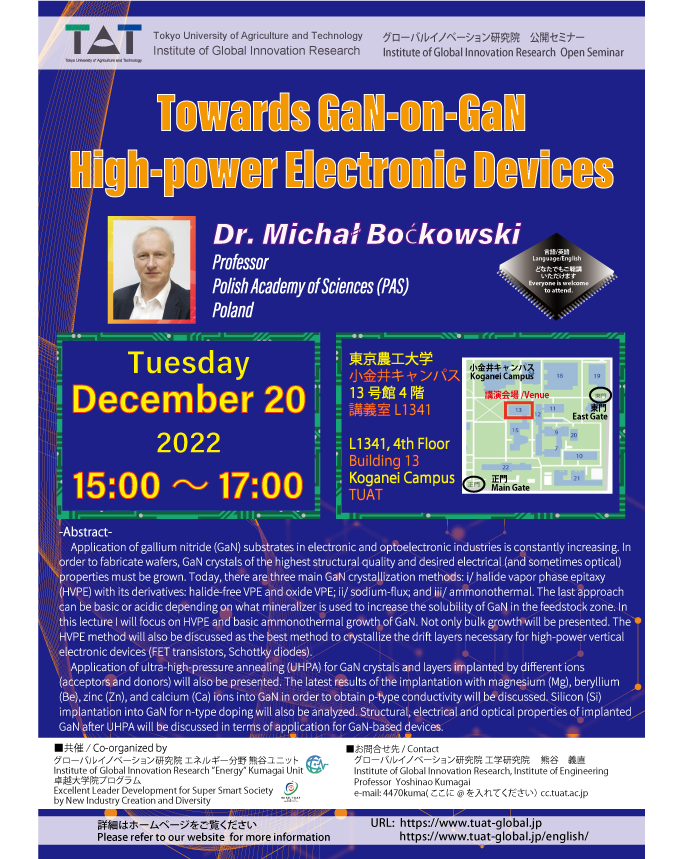
| 日時 | 2022.12.20(15:00~17:00) |
|---|---|
| 会場 | |
| 講演者 | Dr. Michał Boćkowski |
| 所属機関 | ポーランド科学アカデミー (ポーランド) |
| 講演タイトル | "Towards GaN-on-GaN High-power Electronic Devices" <要旨> Application of gallium nitride (GaN) substrates in electronic and optoelectronic industries is constantly increasing. In order to fabricate wafers, GaN crystals of the highest structural quality and desired electrical (and sometimes optical) properties must be grown. Today, there are three main GaN crystallization methods: i/ halide vapor phase epitaxy (HVPE) with its derivatives: halide-free VPE and oxide VPE; ii/ sodium-flux; and iii/ ammonothermal. The last approach can be basic or acidic depending on what mineralizer is used to increase the solubility of GaN in the feedstock zone. In this lecture I will focus on HVPE and basic ammonothermal growth of GaN. Not only bulk growth will be presented. The HVPE method will also be discussed as the best method to crystallize the drift layers necessary for high-power vertical electronic devices (FET transistors, Schottky diodes). Application of ultra-high-pressure annealing (UHPA) for GaN crystals and layers implanted by different ions (acceptors and donors) will also be presented. The latest results of the implantation with magnesium (Mg), beryllium (Be), zinc (Zn), and calcium (Ca) ions into GaN in order to obtain p-type conductivity will be discussed. Silicon (Si) implantation into GaN for n-type doping will also be analyzed. Structural, electrical and optical properties of implanted GaN after UHPA will be discussed in terms of application for GaN-based devices. |
| 言語 | 英語 |
| 対象 | どなたでも、ご参加いただけます。 |
| 共催 | グローバルイノベーション研究院 エネルギー分野 熊谷義直ユニット 卓越大学院プログラム |
| お問い合わせ窓口 | グローバルイノベーション研究院・工学研究院 熊谷 義直 e-mail: 4470kuma(ここに@ を入れてください) cc.tuat.ac.jp |
| 備考 | 本セミナーは、対面型のみの開催となります。 |
このページの上部へ